Microchip Technology introduced the BodyCom system, a new short-range wireless connectivity technology that uses the capability of the human body to transport a few signals, providing intuitive, simple, and safe communication between two electronically compatible devices.
Communication between BodyCom system devices occurs when they are within a few centimeters of the human body: a simple proximity or touch detection can establish a BodyCom system connection.
The BodyCom system was implemented with the following priorities:
• Very low consumption, especially for the Mobile Unit
• Fast system response
• Stable and Robust communication with Fault detection
• Limited field of action (as little as a few centimeters) to allow an identification when the
touch action takes place from whoever wears the Mobile Unit
• Low cost and complexity
The signal transmission uses capacitive coupling between the human body, the Base Unit and the Mobile Unit (see Figure 1).
Figure 1: BodyCom System Working Principle
Because of this, the signals are more attenuated at low frequencies than at high frequencies, requiring the signals that are transmitted to have higher amplitude for lower frequencies. The Mobile Unit is a battery-powered portable device, and power consumption is a priority, while the Base Unit can deliver more power.
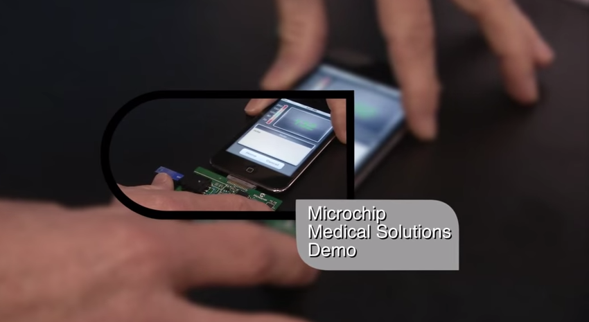
On the video, Applications Engineer Chris Tucker, makes an introduction to BodyCom Technology utilizing the BodyCom Development Kit demonstration.
PIC microcontrollers are finding their way into new applications like Smartphones, Audio Accessories, Video Gaming Peripherals and Advanced Medical Devices.
Microchip provides solutions for the entire performance range of 8-bit microcontrollers, with easy-to-use development tools, complete technical documentation and post design-in support through a global sales and distribution network.
PIC16F1512/13MCUs(28-Pin Flash Microcontrollers with XLP Technology) combine eXtreme low-power technology and high digital & analog peripheral integration for use in a wide variety of applications. Check the short presentation below by Primo Castro (Product Marketing Manager at Microchip) and learn about the details on this Data Sheet.
The board integrates an MPU-6050motion sensing chip from InvenSense. The MPU-6050 has a 3-axis gyroscope, 3-axis accelerometer and uses sensor fusion technology to create a 3-D reference frame.
Microchip’s Motion Sensor Demo Board allows you to easily add this breakthrough technology to your next gaming accessory, tabletPC, digital camera, robotic component, or any other consumer application.
The Spizzle Demo is actually a PC gaming application where you rotate a spherical puzzle and try to line it up for the approaching/matching pieces.
The MCP3911 is a 2.7V to 3.6V dual channel Analog Front End (AFE) containing two synchronous sampling Delta-Sigma Analog-to-Digital Converters (ADC), two PGAs, phase delay compensation block, internal voltage reference, modulator output block, and highspeed 20 MHz SPI compatible serial interface.
The MCP3911 is capable of interfacing a large variety of voltage and current sensors including shunts, current transformers, Rogowski coils and Hall effect sensors.
The video below presents a brief introduction to the MCP3911 Analog Front-End and reviews the MCP3911 ADC Evaluation Board for 16-bit MCUs for high accuracy energy measurement and data acquisition applications.
Learn more at Microchip. Please share this article with your social circles and show your support. If you want to get future updates to your email inbox or feed reader then kindly subscribe on our RSS feed and Newsletter. Do not miss also our trending news and tweets for today!
As more electronic applications require low power or battery power, energy conservation becomes paramount.
Today’s applications must consume little power, and in extreme cases, last for up to 15-20 years, while running from a single battery.
To enable applications like these, products with Microchip’snanoWatt XLP Technology offer the industry’s lowest currents for Run and Sleep, where extreme low power applications spend 90%-99% of their time.
It’s the perfect solution to those looking for a low-cost, easy-to-use development platform.
All Microstick kits are USB-powered and include an on-board debugger/programmer, a Device Under Test (DUT socket) for easy device swapping, a user LED and reset button.
These kits are designed for insertion into a standard prototyping board for easy connection to additional circuitry.
The kits are extremely portable as well and is still about the size of a stick of gum!
Key Features :
- Low Cost
- Integrated USB programmer / debugger - No external debugger required
- USB Powered - Ease of use, No external power required
- MPLAB support.
- DUT Socket - Flexible, Easy device replacement
- 0.025” Pin headers - Enables plug-in to Breadboard with room for jumper wires
- Easy access to all device signals for probing
- Small size - Smaller than a stick of gum at 20 x76mm (approx) - Easily Portable
Subscribe on our Newsletters for future updates to your email inbox or feeds reader. Share our article and help us to spread our voice. Feel free to comment below what you think.
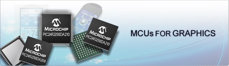
Howdy folks? Today we share with you an easy and cost-effective graphics solution from Microchip Technology.
Microchip's 16-bit, PIC24 MCUs and dsPIC® Digital Signal Controllers provide designers with an easy upgrade path from 8-bit PIC® microcontrollers and a cost effective option to 32-bit MCUs.
The broad product line includes everything from eXtreme Low Power microcontrollers to high performance digital signal controllers.
I've been looking for an application like this for my car display. I'd love to replace my rocker switch panel with a touch screen display. What about you?
On display at Microchip's Design West booth were several of Microchip's digital power reference designs, including the solar micro inverter, LLC resonant converter, quarter brick DC/DC and LED development board.
More on the video below :
You liked our post? Then kindly share it with your friends and show your support. Subscribe on our RSS feed and stay tuned for more!
Microchip's advanced motor control solutions in action at ESC! A dsPIC digital signal controller controls a BLDC motor, an AC induction motor, and a stepper motor using high performance motor control techniques.
Time flies when you're having fun, but it goes by even faster when you're creating the future. This short video from Brian Krzanich's 2012 Intel International Sales and Marketing Conference keynote shows just how much they've created in 44 years.
The Overhead Console demo features the usage of Microchip's mTouch™ technology in a capacitive touch sensing application in an automotive module. A single, cost effective PIC18F66K80 microcontroller is the cornerstone of this demo featuring 11 capacitive touch inputs with various styles of touch pads housed in a module with class "A" curved surfaces.
RGB LED lighting is used for backlighting the touch pad graphics. LIN and CAN communication protocols are supported.
The unique electrical properties of graphene have enticed researchers to envision a future of fast integrated circuits made with the one-carbon-atom-thick sheets, but many challenges remain on the path to commercialization. Scientists from the University of Florida have recently tackled one of these challenges - how to reliably manufacture graphene on a large scale.
The team has developed a promising new technique for creating graphene patterns on top of silicon carbide (SiC). SiC comprises both silicon and carbon, but at high temperatures (around 1300 degrees Celsius) silicon atoms will vaporize off the surface, leaving the carbon atoms to grow into sheets of pure graphene. Researchers had previously used this thermal decomposition technique to create large sheets of graphene, which were then etched to make the patterns required for devices.
The etching process, however, can introduce defects or chemical contaminants that reduce graphene's prized electron mobility. In contrast, the Florida team's technique allowed the researchers to confine the growth of graphene to a defined pattern as small as 20 nanometers. The team found that implanting silicon or gold ions in SiC lowered the temperature at which graphene formed by approximately 100 degrees Celsius. The team implanted ions only where graphene layers were desired, and then heated the SiC to 1200 degrees Celcius.
At this temperature the pure SiC did not form graphene, but the implanted areas did. Using this technique, the team successfully created graphene nanoribbons, thin lines of graphene with nanoscale dimensions. With further refining, the process, described in the AIP - American Institute of Physics' journal, Applied Physics Letters, may be able to encourage selective graphene growth at even lower temperatures, the researchers write.
You knowIntel as world-class top microprocessor company, but what do you know about the making of a chip? Our guest blogger, Rob Kelton from Intel’s Internal Employee Communications team, walks us through the making of the microprocessor, the brain "behind the magic" of your PC.
Microprocessors have been called the most complex manufactured product on earth, created through hundreds of steps in an ultra-clean environment. A few years ago we shared a picture story of chip manufacturing on 45-nanometer (nm) process technology and now we’d like to share an updated version that includes our 22 nm and Tri-gate transistor technology (not every single step, but most of the important ones).
Silicon is the second most abundant element in the earth’s crust. Common sand has a high percentage of silicon. Silicon - the starting material for computer chip - is a semiconductor, meaning that it can be readily turned into an excellent conductor or an insulator of electricity, by the introduction of minor amounts of impurities.
Melted Silicon
In order to be used for computer chips, silicon must be purified so there is less than one alien atom per billion. It is pulled from a melted state to form a solid which is a single, continuous and unbroken crystal lattice in the shape of a cylinder, known as an ingot.
A mono-crystal silicon ingot has a diameter of 300 millimeters (mm) and weighs about 100 kilograms (roughly 220 pounds).
Ingot Slicing
The ingot is cut into individual silicon discs called wafers. Each wafer has a diameter of 300mm and is about 1 mm thick. Wafers are polished until they have flawless, mirror-smooth surfaces. Intel buys manufacturing-ready wafers from its suppliers. Wafer sizes have increased over time, resulting in decreased costs per chip. When Intel began making chips, wafers were only 50mm in diameter. Today they are 300mm, and the industry has a plan to advance to 450mm.
Fabrication of chips on a wafer consists of hundreds of precisely controlled steps which result in a series of patterned layers of various materials one on top of another.
What follows is a sample of the most important steps in this complex process.
Applying Photo Resist (Wafer Level)
Photolithography is the process by which a specific pattern is imprinted on the wafer. It starts with the application of a liquid known as photoresist, which is evenly poured onto the wafer while it spins. It gets its name from the fact that it is sensitive to certain frequencies of light (“photo”) and is resistant to certain chemicals that will be used later to remove portions of a layer of material (“resist”).
Exposure
The photoresist is hardened, and portions of it are exposed to ultraviolet (UV) light, making it soluble. The exposure is done using masks that act like stencils, so only a specific pattern of photoresist becomes soluble. The mask has an image of the pattern that needs to go on the wafer, it is optically reduced by a lens, and the exposure tool steps and repeats across the wafer to form the same image a large number of times.
Resist Development
The soluble photoresist is removed by a chemical process, leaving a photoresist pattern determined by what was on the mask.
Ion Implantation
The wafer with patterned photoresist is bombarded with a beam of ions (positively or negatively charged atoms) which become embedded beneath the surface in the regions not covered by photoresist. This process is called doping, because impurities are introduced into the silicon.
This alters the conductive properties of the silicon (making it conductive or insulating, depending on the type of ion used) in selected locations. Here we show the creation of wells, which are regions within which transistors will be formed.
Removing Photo Resist
After ion implantation, the photoresist is removed and the resulting wafer has a pattern of doped regions in which transistors will be formed.
Begin Transistor Formation
Here we zoom into a tiny part of the wafer, where a single transistor will be formed. The green region represents doped silicon.
Today’s wafers can have hundreds of billions of such regions which will house transistors.
Etch
In order to create a fin for a tri-gate transistor, a pattern of material called a hard mask (blue) is applied using the photolithography process just described. Then a chemical is applied to etch away unwanted silicon, leaving behind a fin with a layer of hard mask on top.
Removing Photoresist
The hard mask is chemically removed, leaving a tall, thin silicon fin which will contain the channel of a transistor.
Silicon Dioxide Gate Dielectric
Using a photolithography step, portions of the transistor are covered with photoresist and a thin silicon dioxide layer (red) is created by inserting the wafer in an oxygen-filled tube-furnace. This becomes a temporary gate dielectric.
Polysilicon Gate Electrode
Again using a photolithography step, a temporary layer of polycrystalline silicon (yellow) is created. This becomes a temporary gate electrode.
Insulator
In another oxidation step, a silicon dioxide layer is created over the entire wafer (red/transparent layer) to insulate this transistor from other elements.
Intel uses a “gate last” (also known as “replacement metal gate”) technique for creating transistor metal gates. This is done in order to avoid transistor stability problems which otherwise might arise as a result of some subsequent high temperature process steps.
Removal of Sacrificial Gate
Using a masking step, the temporary (sacrificial) gate electrode and gate dielectric are etched away. The actual gate will now be formed; because the first gate was removed, this procedure is known as “gate last”.
Applying High-k Dielectric
Individual molecular layers are applied to the surface of the wafer in a process called “atomic layer deposition”. The yellow layers shown here represent two of these. Using a photolithography step, the high-k material is etched away from the undesired areas such as above the transparent silicon dioxide.
Metal Gate
A metal gate electrode (blue) is formed over the wafer and, using a lithography step, removed from regions other than where the gate electrode is desired.
The combination of this and the high-k material (thin yellow layer) gives the transistor much better performance and reduced leakage than would be possible with a traditional silicon dioxide/polysilicon gate.
Ready Transistor
This transistor is close to being finished. Three holes have been etched into the insulation layer (red color) above the transistor. These three holes will be filled with copper or other material which will make up the connections to other transistors.
Electroplating
The wafers are put into a copper sulphate solution at this stage. The copper ions are deposited onto the transistor thru a process called electroplating. The copper ions travel from the positive terminal (anode) to the negative terminal (cathode) which is represented by the wafer.
After Electroplating
On the wafer surface, the copper ions settle as a thin layer of copper.
Polishing
The excess material is mechanically polished away to reveal a specific pattern of copper. Multiple metal layers are created to interconnect (think: wires) all the transistors on the chip in a specific configuration. How these connections have to be “wired” is determined by the architecture and design teams that develop the functionality of the respective processor (e.g. Intel® Core™ i5 Processor ).
While computer chips look extremely flat, they may actually have over 30 layers to form complex circuitry. A magnified view of a chip will show an intricate network of circuit lines and transistors that look like a futuristic, multi-layered highway system.
After all the interconnect layers are formed, an array of solder bumps is put on each die. These are the electrical connections with which the chip will communicate with the outside world, through the package in which it is later inserted. (These bumps are not shown in the illustrations). When wafer processing is complete, the wafers are transferred from the fab to an assembly/test facility.
There, the individual die are tested while still on the wafer, then separated, and the ones that pass are packaged. Finally, a thorough test of the packaged part is conducted before the finished product is shipped.
Wafer Sort
This portion of a ready wafer is being put through a test. A tester steps across the wafer; leads from its head make contact on specific points on the top of the wafer and an electrical test is performed. Test patterns are fed into every single chip and the response from the chip is monitored and compared to “the right answer”.
Wafer Slicing
The wafer is cut into pieces (called die). The above wafer contains future Intel processors codenamed Ivy Bridge.
Selecting Die for Packaging
The die that responded with the right answer to the test patterns will be packaged.
Individual Die
Like this one, have been cut out in the previous step (singulation). The die shown here is Intel’s first 22nm microprocessor codenamed Ivy Bridge.
Packaging
The package substrate, the die and the heat spreader are put together to form a completed processor. The green substrate builds the electrical and mechanical interface for the processor to interact with the rest of the PC system. The silver heat spreader is a thermal interface which helps dissipate heat.
Processor
Completed processor (Ivy Bridge in this case). A microprocessor has been called the most complex manufactured product made by man.
In fact, it takes hundreds of steps - only the most important ones have been included in this picture story - in the world’s cleanest environment (a microprocessor fab).
Class Testing
During this final test the processor is thoroughly tested for functionality, performance and power.
Binning
Based on the test result of class testing, processors with equal capabilities are binned together in trays, ready for shipment to customers.
Retail Package
Manufactured and tested processors are shipped to system manufacturers in trays or to retail stores in a box (the box shown is actually the box of a 32nm product and not the actual box for our 22nm Ivy Bridge products).
BONUS: Here’s a PDF presentation of this article that you can share with family and friends. If you need a PowerPoint version for training purposes, contact Markus Weingartner. You can also find a video, photos, and other useful presentations of “The Making of a Chip” in Intel's Press Kit.
(DISCLOSURE: This page contains affiliate links. If you purchase a product through one of them, I will receive a commission (at no additional cost to you). I only ever endorse products that I have personally used and benefitted from personally. Thank you for your support!)
Scientists have built the world's tiniest transistor by precisely positioning a single phosphorus atom in a silicon crystal. The nano device is an important step in the development of quantum computers – super-powerful devices that will use the weird quantum properties of atoms to perform calculations billions of times faster than today's computers.
Michelle Simmons, of the University of NSW (New South Wales), said single atom devices had only been made before by chance and their margin of error for placement of the atom was about 10 nanometres, which affected performance. Her team was the first to be able to manipulate individual atoms with "exquisite precision".
Using a technique involving a scanning tunnelling microscope, they were able to replace one silicon atom from a group of six with one phosphorus atom, achieving a placement accuracy of better than half a nanometre. "This device is perfect," Professor Simmons, director of the Australian Centre of Excellence for Quantum Computation and Communication Technology, said.
The single atom sits between two pairs of electrodes, one about 20 nanometres apart, the other about 100 nanometres apart. When voltages were applied across the electrodes, the nano device worked like a transistor, a device that can amplify and switch electronic signals.
First developed in the 1950s, transistors revolutionised the electronics industry. Since then, miniaturisation has seen the number of transistors squeezed onto a circuit double about every two years – a trend known as Moore's law.
Professor Simmons said this led to the prediction that transistors would need to reach the single atom level by 2020. "So we decided 10 years ago to start this program to try and make single atom devices as fast as we could, and try and beat that law." This had now been achieved eight to ten years ahead of the industry's schedule, she said.
Last year, Professor Simmons was named NSW Scientist of the Year for her team's research.
About 15 to 20 years of research is needed before quantum computers become widely available.
At the end of September we found out that until 2011 ended, AMD planned to launch two new chips in its A-Series APU product family which were supposed to come with unlocked multiplier, dubbed the A6-3670K and A8-3870K, and these two processors have now become available for pre-order in the US.
Both of these processors greatly resemble their predecessors, the A8-3870K coming as a 100MHz higher clocked version of the current A8-3850, which means that it now runs at 3GHz.
The second unlocked APU to be released by AMD is called the A6-3670K and this also is an almost exact copy of the A6-3650 it is meant to replace apart from the 2.7GHz operating speed, again 100MHz higher than that of its predecessor.
Outside of the higher operating clock and unlocked multiplier, both of these chips will feature similar specifications as they sport quad processing cores with 4MB of Level 2 cache memory, an integrated dual-channel DDR3-1866MHz controller, and built-in Radeon HDgraphics.
The power consumption of the two AMD accelerated processing units was also left untouched which means that is rated at 100W.
Pre-order prices of the AMD A-Series 3670K and 3870K APUs listed by Bottom Line Telecommunications and uncovered by CPU-World are set at $121.50 (90.6 EUR) and $143.77 (107.25 EUR).
On a quick look, these seem to be identical with what the current A6-3650 and A8-3850 chips are retailing for in the same store, so there is a strong possibility that AMD will introduce the new APUs at the same price level as their current counterparts.
The unlocked multiplier design that AMD plans to introduce with the 3670K and 3870K will greatly improve their overclocking potential since the maximum FSB achieved by Llano APUs is severely limited at this point, mostly due the integrated graphics core.
Read also other related AMD topics and comment below what do you think about our post. Spread the word about it!
Think you have what it takes to turn a hot idea into a cool solution? Then Circuit Cellar and Elektor, in association with DesignSpark, would like to cordially invite you to participate in the DesignSpark chipKITTM Challenge!
Starting November 28, engineers from around the world are challenged to develop an energy-efficient and eco-friendly design solution using DesignSpark’s free PCB software and Microchip Technology’s chipKITTMMax32TM development board. Achieve the most energy-efficient solution and you could win share of $10,000! Maximize your design power while reducing your environmental and energy footprint.
Entries must :
Be developed using the Microchip chipKITTM development board
Include an extension card developed using DesignSpark's PCB tools
Compile using Microchip's MPIDE software
Your prize-winning, efficient application can be anything that reduces the energy footprint of a system -a controller for a windmill, an energy-efficient battery charger or even a piece of hardware that lets you drive your e-bike miles farther! Entries will be judged on their level of energy efficiency and the quality of the extension card's PCB design.
Plus, keep the DesignSpark community regularly informed through posts on the DesignSpark Project Pages and your updates will make you eligible for Community Choice Awards and random prize drawings! Win $100 vouchers for Allied Electronics and RS Components as well as free subscriptions to Circuit Cellar and Elektor magazines.
DesignSpark, in participation with Microchip Technology, has made 1000 sample kits available for the competition. Sign up nowto see if you qualify for a free chipKITTM Max32TM development board. All chipKITM Max32TM users are encouraged to participate.
The deadline for submission is 13.00 EST / 19.00 CET, March 27, 2012.
How to Dress for Success Wondering what is the appropriate business outfit for success? Here are some tips on how to dress and look professional. Weekly Promotion