7 Reasons to Consider a Home Gym

If you think of picking up better health habits and don't like crowded gyms, consider setting a home gym catered to your needs.

5 Top Picks for Christmas Holiday Like a Fairytale

If you imagine Christmas holiday this year being like a fairytale, you should consider visiting these hidden gems!

7 Fashion Accessories To Lift Up Your Style Quotient

Get heads up on the trendiest as well as classic fashion accessories that would elevate your style to another level.

Sensibo

Showing posts with label Microprocessors. Show all posts

Our Selection of the Top 10 Devices Revealed at CES 2014 Mega - Event

Description :

Hello Brothers & Sisters entire world. Enjoy your days in this blessed week. Not sure what you're after, but we hope the rest of your day is good. 😃

Thanks to you, THE OFFICIAL ANDREASCY is continuously growing! Do you want to shape the future with us? We are currently conducting a survey and we'd appreciate if you share your valuable feedback. The survey will only take a few minutes. Please, help us to serve you better! 

If you enjoy our blog site, then you know it, if it's Tech it's here. And today, we bring you the future. We dive into CES 2014, the Gigantic Tradeshow event (Location: Las Vegas, USA) and we present the Hottest New Technology gadgets around. 

The Best of CES 2014

Another year, another Consumer Electronics Show has come and gone, and our editorial team picks the best devices that hit the show floor. Some truly interesting innovations, including Smart Watches, Gaming hardware, PC Concepts, TVs, and more.

So what are we waiting for? Let's get to know the Top 10 Devices from this year's event. With a drum roll, ladies and gentlemen, here is the honour list:

1. Pebble Steel Smartwatch

Now hand watches do better than showing time, date, stopwatch and alarms. Pebble Watch came at CES with a new metallic version called "Pebble Steel Smartwatch".

Pebble Steel Smartwatch

Still supporting Android and iOS, this version includes Corning Gorilla Glass, protecting the E-lnk screen. The battery of the watch was created to last for a week. It's price is $249 and is going to be available from January 28, 2014.

2. Oculus Rift Crystal Cove

The 3D headset for gamers has been improved: Oculus VR revealed its new prototype for Oculus Rift, code-named "Crystal Cove".

Oculus Rift Crystal Cove

This model includes small infrared LEDs on the front surface of the headset. These LEDs that look like white dots emit signals that a camera captures, similar to a webcam. By the way, the graphics are more detailed: Crystal Cove can refresh much faster the information displayed (every 1 to 2 milliseconds compared to 16 milliseconds from the previous model).

3. Project Christine

Here is an interesting concept PC, perfect for huge RTS (real-time strategy) games like League of Legends or StarCraft II. "Project Christine" is a bold re-imagining of the modern desktop with a modular design, made by Razer, a not very large company that develops and sells devices for gamers.

Project Christine

Christine comes with this fascinating design, and several modules like CD/DVD drives, Hard Disk Drives, GPU, RAM Memory etc. Users can customize or upgrade the PC by simply changing the modules on the central tower in order to have a better gaming experience. You can even hot swap the power supply!

4. PlayStation Now

Two months after the release of the PlayStation 4, Sony unveiled it's cloud service "PlayStation Now". Players were waiting for this since 2012, after the acquisition of Gaikai, a company which provides technology for the streaming of high-end video games.

PlayStation Now

We don't have a release date for the moment, however we know that the service will be compatible with PS4, PS Vita and maybe with smartphones, tablets and TVs. Also it will allow users to play PS3 games (and PS2?) without installing the games on the console.

5. LG’s Curved TV

The key number of this TV by LG is 105. Actually 105 inches for the LG Curved Ultra HD TV, with a 21:9 screen.

LG’s Curved TV

The advantage of this curved TV is it's viewing angle. The viewing angles are as wide as you like and the picture is extremely clear from virtually any perspective. By the way, LG, knowing that there'll be a little number of adopters, also made a 65-inch version. Simply awesome!

6. Samsung Galaxy Note Pro 12.2

We wonder how Samsung was inspired for it's Galaxy Note Pro tablet: you just have to see the home screen to say that it reminds a bit Windows 8 Modern UI (Metro).

Samsung Galaxy Note Pro 12.2

Going by the specs this lightweight (759gr) 12.2 - inch tablet, measures 7.95 mm thick. It comes with Android 4.4 KitKat, and offers a huge display resolution of 2560x1600 (pixels), 3 Gb of RAM, and a huge Exynos 5 Octa chip plus a combined 1.9 GHz Quad Core and a 1.3 GHz Quad Core processor. And it's performance doesn't stop here.

7. Parrot MiniDrone

Star of the CES 2014, the Parrot MiniDrone, a quadricopter that received several awards including an Innovation Award in the category "Wireless Handset Accessories".

Parrot MiniDrone

The MiniDrone works by being connected to a smartphone or a tablet using Bluetooth Smart. With it's ultra compact design, it can do high speed flights, do acrobatics with great precision and climb along walls with two ultralight wheels. This thing can really fly...

8. EyeLock Myris Iris Scanner

Forget fingerprints! Between DNA and Technology, there is Eyelock Myris, a USB iris scanner device, which has an arguably better take on biometric security. Pick it up, flip it over, look at it, and the sensor will scan your eye to verify your identity. It can work with your PC, Mac or Chrome OS.

EyeLock Myris Iris Scanner

Better than using passwords! Myris allows you to protect your digital life while making it more easily accessible. Thank you DNA!

9. Nvidia Tegra K1 Processor

It also had it's say at CES. Nvidia unveiled Tegra K1 Processor, having 192 GPU cores and 4 Gb of Memory.

Nvidia Tegra K1 Processor

The processor brings huge graphics performances from PCs or consoles to tablets and smartphones. It allows for example to play PC or console games on Android, with an amazing graphics rendering. The 32 bit version will be released on the first half of 2014.

10. Makerbot Z18 Industrial 3D Printer

As we talk a bit more about 3D printing, Makerbot revealed it's Replicator Z18 which is definitively a beast of a 3D printer.

Makerbot Z18 Industrial 3D Printer

Even if it's cost is huge ($6,499), the Replicator Z18 3D Printer allows prints up to 12x12x18 inches (about 30x30x45 cm). According to Bre Pettis, CEO of Makerbot Industries, "this is industrial-strength 3D printing".

With that we're closing the curtains on CES 2014. We hope you liked our selection. Please take our poll on the best devices below, and leave a comment about your own opinion.

What was the best gadget of CES?
  
pollcode.com free polls 

Learn about the latest happenings on Social Media, news and comments, plus tips on using Facebook and other web social tools.

Thank you all for your support! Have a productive week. 😎💓

*by andreascy*

David C. Brock: The Chemical History of Electronics

Description :

The rise of semiconductor electronics is one of the most important developments in recent history. The manufacture of semiconductor devices relies fundamentally on chemical processes, equipment, and specially produced materials. 

David C. Brock: The Chemical History of Electronics

David C. Brock is a senior research fellow with CHF's Center for Contemporary History and Policy. As a historian of science and technology, he specializes in the history of semiconductor science, technology, and industry; the history of instrumentation; and oral history. He is the author of Understanding Moore's Law: Four Decades of Innovation and, with Christophe Lécuyer, Makers of the Microchip: A Documentary History of Fairchild Semiconductor (Acquired by Onsemi).

In this history of chemistry webisode, David Brock talks about the history of how the microprocessors that power iPads, iPhones and other digital devices came about. An excellent presentation! 


RELATED TOPIC: From Sand to Silicon : The making of Intel microprocessors

You could bring forward your opinions and suggestions and let us know what you think. If you like this post then it's about time to get our content. If you enjoy our news then feel free also to subscribe on our RSS feed and check out some of the latest Trending News and Tweets tailored for you.

*by andreascy*

Go Wireless with Renesas WiFi Out-of-the-Box Solutions


Description : 

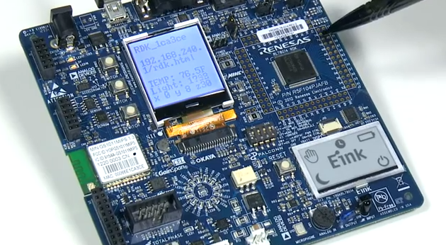
Renesas Electronics the world's number one supplier of flash microcontrollers and advanced semiconductor solutions, presents RL78/G14 RDK kit. This kit features an integrated Wi-Fi utilities to provide a simple yet powerful mean to configure the WI-FI settings of this demonstration kit, define point to point Wi-Fi connections, run in a web server mode and connected to external clouds. 


Three presenters from Renesas Electronics Americas and from Gainspan Corp. are taking turn to introduce the feature of this new kit and all live sensor data feed can be transmitted over Wi-Fi. Alternately, it is shown how to :

  • Connect to the embedded Web Server and read sensor data
  • How to launch and run smartphone applications (iPhone or iPad or Android phones) and do the same thing.


Renesas low power RL78/G14 demo kit gives customers exciting off-the-shelf building blocks to quickly prototype and create their own Wi-Fi cloud-connected M2M products. Customers can evaluation Wi-Fi connectivity and multiple connection modes with this low-cost demonstration kit.


For more information and to purchase a kit go here. Discover other Electronic related stories and  stay updated by subscribing to our News feeds. Comment below or send us your suggestions for the future.

*by andreascy*

3 Creative Raspberry Pi Projects

Description : 

A Raspberry Pi is a single-board computer i.e. it has a processor, R.A.M, I/O and other features that a computer is required to have on a single circuit board. It does not have a long term memory of its own so instead it uses a SD card for that purpose. 

3 Creative Raspberry Pi Projects

The Raspberry Pi is extensively used in portable appliances. Moreover, since it is programmable and can control devices, it can be moulded in to some very exciting gadgets. Herein you will find some creative examples of using a raspberry pi in some cool projects.

1. Control Things Around The Home With Remote Control Raspberry Pi

What is better than controlling all the appliances in the house without getting up from your comfortable sofa? Just imagine how annoying it is to wake up in the morning and realise you left the lights and the fan on, or when someone asks you to turn off the water pump in the lawn while you are watching an intense major league baseball match. That hurts big-time! 

3 Creative Raspberry Pi Projects

Here is the solution to all such ‘getting up and do work’ problems. Thanks to the miniaturized computer, and a simple combo of hardware cum software, you can sit back and relax all day long with your remote control, cleverly avoiding trivial work stuff. For this project items needed are :

       - Raspberry pi

      - Programmable remote control

      - Remote control switches

      - Lego pieces (to make your Raspberry Pi look cool) 

2. Remote Control Raspberry Pi Boat Another interesting idea is a remote control boat 

There’s no need to mention how much fun you can have with a project of this type playing with it in a local pond or swimming pool.This might be considered a project for the big kids, but the reality is that engineers are working on a drone water vessel called FishPi to sail on the Atlantic Ocean and collect data. So it may not be long before there is a prototype model for this project. 

3 Creative Raspberry Pi Projects

 How a motor can be controlled by a Raspberry Pi? For this purpose a USB controlled motor driver is necessary and it needs to be configured to the projects needs. Other than the controller, two small DC motors are needed; one for the propeller and the other for controlling the direction of the propeller. The wattage of motors depends on how large the vessel is going to be. You can command the direction of the boat using a low-profile Wi-Fi dongle but the key component is of course the Raspberry Pi. 

 3. Physical Gmail Notifier 

Now there’s no need to be in front of the PC to know that a new email has arrived. Get notified about the newly received mail through the physical email notifier. All this cool gadget needs is :

       - An LED

       - A GPIO(General Purpose Input/Output) module 

       - Internet enabled raspberry pi 

       - Software required : Python 

Configure GPIO with one Gmail account using Python, with GPIO-pin status as true if email is received, else status should be false. Connect GPIO output pins with terminals of LED. The LED will glow if a new inbox message has been received. 

3 Creative Raspberry Pi Projects

 Of course some intricate electronic components are involved in each of these projects but as they say, “Well begun is half done” and projects begin with ideas. It doesn’t end here…you too can think of some creative ideas and with some effort you can achieve something great. Just a little brain storming is needed and you’re off! 

We managed to get a Raspberry Pi computer on its first release in February from Premier Farnell Element 14. This has kicked off an avid obsession into exploring its capabilities and the creativity of others in the Raspberry Pi community.

*by andreascy*

Intel® vPro Technology : Environmental Pre-requisites

Description :

This module discusses the various pre-requisites that ease the setup and configuration process of Intel® vPro™ Technology clients.


Check also :

Instant back to work with Intel Core vPro processors

Cummins PowerShell GUI

*by andreascy*

Intel® Anti-Theft Technology helps deter data and asset theft

Description :

This is a fun video for usage in social media showing one way Intel® Anti-Theft Technology helps protects a consumer's laptop asset and their data. 


Intel Anti-Theft Technology is available on all 3rd generation Intel® Core™ enabled Ultrabooks and on select Intel Core enabled laptops.


*by andreascy*

HP : Product Manager Greg Morris presents New Desktops for Business

Description :

HP recently unveiled its newest Professional Desktops that keep employees productive and provide Professional Innovations to manage and help protect Businesses.


*by andreascy*

Samsung All-in-one PC SERIES 9 hands on video

Description :

The new Samsung All-in-one PC SERIES 9 offers a brilliant entertainment experience with immersive 3D technology, an ultra-clear yet super-thin 27" full HD display, and high quality sound optimized by JBL. 


In addition, the blistering power of the 2nd generation Intel Core i7 processor and on-board AMD Radeon graphics ensure you have all the processing and video power you'll need. 


*by andreascy*

Financial Services Solutions from IBM and Intel Xeon E5 Processor

Description :

NYC Public Library : Dave Weber (IBM) discusses IBM solutions for the financial services industry including innovations around improved throughput, low latency, and increased memory capacity.


 IBM and Intel have worked together to improve Reliability and Scalability (RAS) within the x86 architectures. 


*by andreascy*

Cisco Announces new servers with Intel Xeon E5 Processor Family

Description :

NYC Public Library : Scott Ciccone (Cisco) talks about Cisco's 3rd generation of unified management, fabric interconnect, and fabric extenders. 


Watch as Scott describes the features of the 3rd generation of fabric computing innovations, based on the Xeon E5 2600 processor including the UCS rack and blade servers. 


*by andreascy*

Intel - How Far We've Come (1968-2012)

Description :

Time flies when you're having fun, but it goes by even faster when you're creating the future. This short video from Brian Krzanich's 2012 Intel International Sales and Marketing Conference keynote shows just how much they've created in 44 years. 


Homepage

*by andreascy*

Instant Back to Work with Intel Core vPro processors

Description :
How do you minimize end user downtime when they experience system errors? Deploy PCs with Intel Core vPro processors that allow IT to remotely diagnose, repair, and patch PCs remotely, all while the end user continues to be productive via temporary image. 


*by andreascy*

Beat Intel, Get Your 14 nm Process Development Kit Now!

Description :
The industry’s first process development kit (PDK) for 14nm logic chips has been announced by Imec. This early-version PDK contains all elements for design assessment of the 14nm node through device compact models, parasitic extraction, design rules, parameterized cells (pcells), and basic logic cells. 


It anticipates the introduction of a number of new technologies like the use of FinFET transistors, which have a larger drive per unit footprint and higher performance at low supply voltages compared to the traditional planar technologies. Evolutions of this PDK will gradually also introduce the use of high-mobility channel materials. The PDK includes elements of both immersion- and EUV lithography, opening the way for a gradual transition from 193nm immersion to EUV lithography.

Imec releases industry’s first 14nm process development kit

Starting from the PDK a first test chip is now being designed. This chip, planned for the second half of 2012, will allow testing the device-, interconnect-, process- and litho assumptions, as well as performance and power of circuits implemented at the tight area budgets of the 14nm node.

*by andreascy*

From Sand to Silicon: The Making of Intel Microprocessors

Description :

You know Intel as world-class top microprocessor company, but what do you know about the making of a chip? Our guest blogger, Rob Kelton from Intel’s Internal Employee Communications team, walks us through the making of the microprocessor, the brain "behind the magic" of your PC. 

From Sand to Silicon: The Making of Intel Microprocessors

Microprocessors have been called the most complex manufactured product on earth, created through hundreds of steps in an ultra-clean environment. A few years ago we shared a picture story of chip manufacturing on 45-nanometer (nm) process technology and now we’d like to share an updated version that includes our 22 nm and Tri-gate transistor technology (not every single step, but most of the important ones).

Silicon is the second most abundant element in the earth’s crust. Common sand has a high percentage of silicon. Silicon - the starting material for computer chip - is a semiconductor, meaning that it can be readily turned into an excellent conductor or an insulator of electricity, by the introduction of minor amounts of impurities. 

Melted Silicon 

In order to be used for computer chips, silicon must be purified so there is less than one alien atom per billion. It is pulled from a melted state to form a solid which is a single, continuous and unbroken crystal lattice in the shape of a cylinder, known as an ingot.

A mono-crystal silicon ingot has a diameter of 300 millimeters (mm) and weighs about 100 kilograms (roughly 220 pounds).

Ingot Slicing

The ingot is cut into individual silicon discs called wafers. Each wafer has a diameter of 300mm and is about 1 mm thick. Wafers are polished until they have flawless, mirror-smooth surfaces. Intel buys manufacturing-ready wafers from its suppliers. Wafer sizes have increased over time, resulting in decreased costs per chip. When Intel began making chips, wafers were only 50mm in diameter. Today they are 300mm, and the industry has a plan to advance to 450mm.

Fabrication of chips on a wafer consists of hundreds of precisely controlled steps which result in a series of patterned layers of various materials one on top of another.
What follows is a sample of the most important steps in this complex process.

Applying Photo Resist (Wafer Level) 

Photolithography is the process by which a specific pattern is imprinted on the wafer. It starts with the application of a liquid known as photoresist, which is evenly poured onto the wafer while it spins. It gets its name from the fact that it is sensitive to certain frequencies of light (“photo”) and is resistant to certain chemicals that will be used later to remove portions of a layer of material (“resist”). 

Exposure 

The photoresist is hardened, and portions of it are exposed to ultraviolet (UV) light, making it soluble. The exposure is done using masks that act like stencils, so only a specific pattern of photoresist becomes soluble. The mask has an image of the pattern that needs to go on the wafer, it is optically reduced by a lens, and the exposure tool steps and repeats across the wafer to form the same image a large number of times. 

Resist Development

The soluble photoresist is removed by a chemical process, leaving a photoresist pattern determined by what was on the mask.

Ion Implantation 

The wafer with patterned photoresist is bombarded with a beam of ions (positively or negatively charged atoms) which become embedded beneath the surface in the regions not covered by photoresist. This process is called doping, because impurities are introduced into the silicon.

This alters the conductive properties of the silicon (making it conductive or insulating, depending on the type of ion used) in selected locations. Here we show the creation of wells, which are regions within which transistors will be formed. 

Removing Photo Resist 

After ion implantation, the photoresist is removed and the resulting wafer has a pattern of doped regions in which transistors will be formed. 

Begin Transistor Formation

Here we zoom into a tiny part of the wafer, where a single transistor will be formed. The green region represents doped silicon.

Today’s wafers can have hundreds of billions of such regions which will house transistors.

Etch 

In order to create a fin for a tri-gate transistor, a pattern of material called a hard mask (blue) is applied using the photolithography process just described. Then a chemical is applied to etch away unwanted silicon, leaving behind a fin with a layer of hard mask on top. 

Removing Photoresist 

The hard mask is chemically removed, leaving a tall, thin silicon fin which will contain the channel of a transistor.

Silicon Dioxide Gate Dielectric 

Using a photolithography step, portions of the transistor are covered with photoresist and a thin silicon dioxide layer (red) is created by inserting the wafer in an oxygen-filled tube-furnace. This becomes a temporary gate dielectric. 

Polysilicon Gate Electrode 

Again using a photolithography step, a temporary layer of polycrystalline silicon (yellow) is created. This becomes a temporary gate electrode. 

Insulator 

In another oxidation step, a silicon dioxide layer is created over the entire wafer (red/transparent layer) to insulate this transistor from other elements.

Intel uses a “gate last” (also known as “replacement metal gate”) technique for creating transistor metal gates. This is done in order to avoid transistor stability problems which otherwise might arise as a result of some subsequent high temperature process steps.

Removal of Sacrificial Gate 

Using a masking step, the temporary (sacrificial) gate electrode and gate dielectric are etched away. The actual gate will now be formed; because the first gate was removed, this procedure is known as “gate last”. 

Applying High-k Dielectric 

Individual molecular layers are applied to the surface of the wafer in a process called “atomic layer deposition”. The yellow layers shown here represent two of these. Using a photolithography step, the high-k material is etched away from the undesired areas such as above the transparent silicon dioxide. 

Metal Gate 

A metal gate electrode (blue) is formed over the wafer and, using a lithography step, removed from regions other than where the gate electrode is desired.

The combination of this and the high-k material (thin yellow layer) gives the transistor much better performance and reduced leakage than would be possible with a traditional silicon dioxide/polysilicon gate.

Ready Transistor 

This transistor is close to being finished. Three holes have been etched into the insulation layer (red color) above the transistor. These three holes will be filled with copper or other material which will make up the connections to other transistors. 

Electroplating 

The wafers are put into a copper sulphate solution at this stage. The copper ions are deposited onto the transistor thru a process called electroplating. The copper ions travel from the positive terminal (anode) to the negative terminal (cathode) which is represented by the wafer. 

After Electroplating 

On the wafer surface, the copper ions settle as a thin layer of copper.

Polishing 

The excess material is mechanically polished away to reveal a specific pattern of copper. Multiple metal layers are created to interconnect (think: wires) all the transistors on the chip in a specific configuration. How these connections have to be “wired” is determined by the architecture and design teams that develop the functionality of the respective processor (e.g. Intel® Core™ i5 Processor ).

While computer chips look extremely flat, they may actually have over 30 layers to form complex circuitry. A magnified view of a chip will show an intricate network of circuit lines and transistors that look like a futuristic, multi-layered highway system.

After all the interconnect layers are formed, an array of solder bumps is put on each die. These are the electrical connections with which the chip will communicate with the outside world, through the package in which it is later inserted. (These bumps are not shown in the illustrations). When wafer processing is complete, the wafers are transferred from the fab to an assembly/test facility.

There, the individual die are tested while still on the wafer, then separated, and the ones that pass are packaged. Finally, a thorough test of the packaged part is conducted before the finished product is shipped.

Wafer Sort 

This portion of a ready wafer is being put through a test. A tester steps across the wafer; leads from its head make contact on specific points on the top of the wafer and an electrical test is performed. Test patterns are fed into every single chip and the response from the chip is monitored and compared to “the right answer”. 

Wafer Slicing

The wafer is cut into pieces (called die). The above wafer contains future Intel processors codenamed Ivy Bridge. 

Selecting Die for Packaging 

The die that responded with the right answer to the test patterns will be packaged.

Individual Die

Like this one, have been cut out in the previous step (singulation). The die shown here is Intel’s first 22nm microprocessor codenamed Ivy Bridge. 

Packaging 

The package substrate, the die and the heat spreader are put together to form a completed processor. The green substrate builds the electrical and mechanical interface for the processor to interact with the rest of the PC system. The silver heat spreader is a thermal interface which helps dissipate heat. 

Processor 

Completed processor (Ivy Bridge in this case). A microprocessor has been called the most complex manufactured product made by man.

In fact, it takes hundreds of steps - only the most important ones have been included in this picture story - in the world’s cleanest environment (a microprocessor fab).

Class Testing 

During this final test the processor is thoroughly tested for functionality, performance and power. 

Binning 

Based on the test result of class testing, processors with equal capabilities are binned together in trays, ready for shipment to customers. 

Retail Package

Manufactured and tested processors are shipped to system manufacturers in trays or to retail stores in a box (the box shown is actually the box of a 32nm product and not the actual box for our 22nm Ivy Bridge products).


BONUS: Here’s a PDF presentation of this article that you can share with family and friends. If you need a PowerPoint version for training purposes, contact Markus Weingartner. You can also find a video, photos, and other useful presentations of “The Making of a Chip” in Intel's Press Kit.


If you liked our article, kindly share it.


(DISCLOSURE: This page contains affiliate links. If you purchase a product through one of them, I will receive a commission (at no additional cost to you). I only ever endorse products that I have personally used and benefitted from personally. Thank you for your support!)

*by andreascy*

🦾 Stay Motivated

🚀 Tesla Roadster Flies

▶️ Just Press Play

⭐ Leading ShipYard's Leaderboard

🚩 Milestone Unlocked!

🏅 Win-Win