The rise of semiconductor electronics is one of the most important developments in recent history. The manufacture of semiconductor devices relies fundamentally on chemical processes, equipment, and specially produced materials.
David C. Brock is a senior research fellow with CHF's Center for Contemporary History and Policy. As a historian of science and technology, he specializes in the history of semiconductor science, technology, andindustry; the history of instrumentation; and oral history. He is the author of Understanding Moore's Law: Four Decades of Innovation and, with Christophe Lécuyer, Makers of the Microchip: A Documentary History of Fairchild Semiconductor (Acquired by Onsemi).
In this history of chemistry webisode, David Brock talks about the history of how the microprocessors that power iPads, iPhones and other digital devices came about. An excellent presentation!
You could bring forward your opinions and suggestions and let us know what you think. If you like this post then it's about time to get our content. If you enjoy our news then feel free also to subscribe on our RSS feedand check out some of the latest Trending News and Tweets tailored for you.
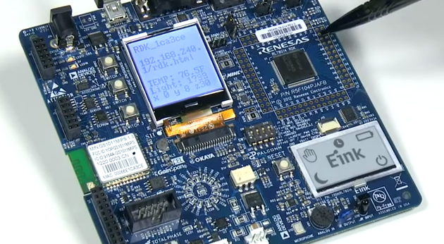
Renesas Electronicsthe world's number one supplier of flash microcontrollers and advanced semiconductor solutions, presents RL78/G14 RDK kit. This kit features an integrated Wi-Fi utilities to provide a simple yet powerful mean to configure the WI-FI settings of this demonstration kit, define point to point Wi-Fi connections, run in a web server mode and connected to external clouds.
Three presenters from Renesas Electronics Americas and from Gainspan Corp. are taking turn to introduce the feature of this new kit and all live sensor data feed can be transmitted over Wi-Fi. Alternately, it is shown how to :
Connect to the embedded Web Server and read sensor data
How to launch and run smartphone applications (iPhone or iPad or Android phones) and do the same thing.
Renesas low power RL78/G14 demo kit gives customers exciting off-the-shelf building blocks to quickly prototype and create their own Wi-Fi cloud-connected M2M products. Customers can evaluation Wi-Fi connectivity and multiple connection modes with this low-cost demonstration kit.
For more information and to purchase a kit go here. Discover other Electronic related stories and stay updated by subscribing to our News feeds. Comment below or send us your suggestions for the future.
With the ever increasing amount of electronics in vehicles, and the demanding nature of high-end and emerging applications, there is a great need for high-speed communications protocols.
Emerging as front-runners for more wide-spread use are:
- FlexRay
- MOST
- Ethernet
The Strategy Analytics Automotive Electronics Service (AES) report, "Automotive High Speed Networks," predicts that Ethernet will see both the fastest growth and the largest volume by 2020. The key breakthrough has been the BroadR-Reach physical layer, from Broadcom, now licensed to other semiconductor vendors, such as NXP. This allows Ethernet at 100 Mbit/s to be transmitted over low-cost, unshielded twisted pair cables.
“Ethernet has gained significant momentum because it meets the requirement for higher-bandwidth bus networks which many feel cannot be met by existing protocols, such as CAN,” stated Ian Riches, Director, Global Automotive Practice.
“FlexRay will continue to find its niche and see volumes grow, but MOST node volumes are likely to start to tail off as we head toward 2020,” added Mark Fitzgerald, Associate Director in the Strategy Analytics Global Automotive Practice.
100 Mbps symmetrical operation using standard Ethernet PHY components (Fig 1)
The OPEN Alliance (One-Pair Ether-Net) Special Interest Group has released their standard for in-vehicle Ethernet over a single twisted pair (Fig. 1). The OPEN Alliance includes two automotive companies, BMW and Hyundai USA, plus three semiconductor companies including Broadcom, Freescale and NXP. BMW will have the first vehicle based on BroadR-Reach technology in 2013.
OPEN fills a gap between CAN, Local Interconnect Network (LIN) and FlexRay that are using automotive control and Media Oriented Systems Transport (MOST), a high-end multimedia network. MOST uses fiber optics and runs at speeds up to 150 Mbits/s. It is a standard 10/100 Mbits/s Ethernet but it uses only a single, unshielded twisted pair cable comparable to that already used by FlexRay. Better yet, it is possible to deliver power over the same two wires like Power-over-Ethernet (POE).
Lower cost of digital camera deployment for advanced driver assist (Fig 3)
The standard defines new PHYs that connect to standard Ethernet MACs. This means that existing microcontrollers with an Ethernet Media Access Controller (MAC) with a Media Independent Interface (MII) can be mated to an OPEN PHY. There are no special drivers or protocols to incorporate. The system works equally well with any standard Ethernet device including those using protocols like IEEE 1588 clock synchronization.
The standard supports the standard Ethernet audio/video bridging (AVB), 802.1BA. It also address temperature and EMC details that are critical to automotive applications. OPEN will be suitable for use anywhere on the car from the engine compartment to doors. Hardware can be qualified for Automotive Electronics Council (AEC) AEC-Q100.
Cable length is limited to 47m. A typical automobile would need no more than a 30m limit but this allows the technology to be used in larger vehicles. The technology can work with significantly longer cables up to about 500m.
Automotive Networking and Consumer Connectivity Applications (Fig 4)
OPEN Ethernet mirrors standard Ethernet that is essentially a switch-based interconnect. This is key because bandwidth is less of an issue assuming a single application can be handled by a link. It is even possible to combine multiple links to provide higher bandwidth but this would be less likely given the drive to use a single cable to reduce costs.
In theory, the new Ethernet approach can reduce connectivity costs by up to 80% and reduces cabling weight by up to 30% compared to a conventional Ethernet LVDS interconnect. OPEN Ethernet can use connectors like those approved for FlexRay. This is important because, at least initially, automotive vendors are likely to use their own approved connectors and cabling.
Still, standard cables and connectors could be useful. For example, a four camera ADAS application would be less expensive if the cameras were a standard component. There is already a standardization effort for automotive cameras. All it would need to incorporate would be a standard OPEN connector. But that is for the future.
Right now the semiconductor participants are delivering chips to handle the new standard. Broadcom's BroadR-Reach family includes a set of PHYs and switches. There are three switches with a mix of built-in PHYs. These include the 7 port BCM89500 with 4 OPEN PHYs, the 7 port BCM89501 with 5 PHYs, and the 4 port BCM89200 with 2 PHYs. The ports without PHYs can be connected to devices or external PHYs. The BCM89810 is a standalone BroadR-Reach 10/100 PHY. This is the PHY that would be used with microcontrollers. In the future, this kind of PHY might be incorporated directly into a microcontroller.
OBD data can be emissions-based or nonemissions-based (Fig 5)
Also part of the mix is Broadcom's BCM89610 10/100/1000 PHY. This is a conventional Ethernet PHY optimized for automotive use. A single BCM89610 could provide a link to an external diagnostic system. The chip has the same EMC resistance as the other BroadR-Reach.
The OPEN Alliance and its members are targeting automotive applications but the technology is ideal for a host of other application areas from robotics to home security systems. Ethernet is already in demand in these applications and a two-wire solution with power easily beats existing technology in cost.
Ethernet has had a long and fruitful life becoming the dominant interconnect for a very wide range of applications. It could now become the dominant interconnect for automotive applications as well.
Have a good day to everyone, follow us we have big informations very soon.
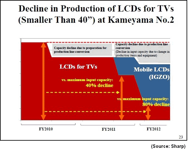
In March 2012 at Kameyama Plant No. 2, Sharp began producing the world’s first high-performance LCD panels incorporating IGZO oxide semiconductors.
Sharp is expanding production scale through April to meet market demand.
Kameyama Plant No. 2 first started operations in August 2006, manufacturing highly advanced LCD panels for TVs.
Production systems have subsequently been reorganized to focus on producing small- and medium-sized LCD panels for the world’s rapidly growing smartphone and tablet terminal markets.
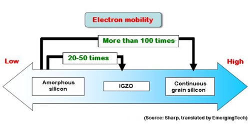
Employing advanced IGZO oxide semiconductors enables Sharp to produce LCDs with smaller thin-film transistors and increased pixel transparency, thus allowing for lower energy consumption.
In addition, proprietary UV2A*3 photo-alignment technology employed in Sharp’s AQUOS LCD TVs enables these displays to achieve high image quality.
Sharp will encourage the application of its new high-resolution LCD panels to high-definition notebook PCs and LCD monitors-which are both expected to grow in demand-as well as to mobile devices. Sharp will also contribute to creating markets for attractive new products.
Sample specifications of LCD Panels incorporating IGZO:
A team of physicists at UCSB (University of California, Santa Barbara) has seen the light, and it comes in many different colors. By aiming high- and low-frequency laser beams at a semiconductor, the researchers caused electrons to be ripped from their cores, accelerated, and then smashed back into the cores they left behind. This recollision produced multiple frequencies of light simultaneously. Their findings appear in the current issue of the science journal Nature.
"This is a very remarkable phenomenon. I have never seen anything like this before," said Mark Sherwin, whose research group made the groundbreaking discovery. Sherwin is a professor of physics at UCSB and a co-author of the paper. He is also director of the campus's Institute for Terahertz Science and Technology.
When the high-frequency optical laser beam hits the semiconductor material - in this case, gallium arsenide nanostructures - it creates an electron-hole pair called an exciton. The electron is negatively charged, and the hole is positively charged, and the two are bound together by their mutual attraction. "The high-frequency laser creates electrons and holes," Sherwin explained. "The very strong, low-frequency free electron laser beam rips the electron away from the hole and accelerates it. As the low-frequency field oscillates, it causes the electron to come careening back to the hole." The electron has excess energy because it has been accelerated, and when it slams back into the hole, the recombined electron-hole pair emits photons at new frequencies.
"It's fairly routine to mix the lasers and get one or two new frequencies, Sherwin continued. "But to see all these different new frequencies, up to 11 in our experiment, is the exciting phenomenon. Each frequency corresponds to a different color."
In terms of real-world applications, the electron-hole recollision phenomenon has the potential to significantly increase the speed of data transfer and communication processes. One possible application involves multiplexing -- the ability to send data down multiple channels - and another is high-speed modulation.
"Think of your cable Internet," explained Ben Zaks, a UCSB doctoral student in physics and the paper's lead author. "The cable is a bundle of fiber optics, and you're sending a beam with a wavelength that's approximately 1.5 microns down the line. But within that beam there are a lot of frequencies separated by small gaps, like a fine-toothed comb. Information going one way moves on one frequency, and information going another way uses another frequency. You want to have a lot of frequencies available, but not too far from one another."
The electron-hole recollision phenomenon does just that - it creates light at new frequencies, with optimal separation between them.
The researchers utilize a free electron laser - a building-size machine in UCSB's Broida Hall -- to produce the electron-hole recollisions, which they note is not practical for real-world applications. Theoretically, however, a transistor could be used in place of the free electron laser to produce the strong terahertz fields. "The transistor would then modulate the near infrared beam," Zaks continued. "Our data indicates that we are modulating the near infrared laser at twice the terahertz frequency. This is where we could really see this working to increase the speed of optical modulation, which is how you get information down a cable line."
The electron-hole recollision phenomenon creates many new avenues for research and exploration, Sherwin noted. "It is an interesting time because there are a lot of people who can participate in doing this kind of research," he said. "We have a unique tool -- a free electron laser -- which gives us a big advantage for exploring the properties of fundamental materials. We just put it in front of our laser beams and measure the colors of light going out. Now that we've seen this phenomenon, we can start doing the hard work of putting the pieces together on a chip."
In discussing the research team's discovery, Sherwin cited Michael Polanyi, the Hungarian scientist and science philosopher. "He talked about growing points in science, and I'm hoping this is going to be one of those, where a lot of people can use it as a foundation for going off in a lot of different directions," he said. "I want to continue working on it, but I'd like to see a lot of other people join in."
Also contributing to the research is the paper's second author, R.B. Liu of The Chinese University in Hong Kong. "This is an excellent example of the value of communicating with scientists from all over the globe," said Sherwin. "If we had never met, this research would not have happened."
Bill takes apart a smoke detector and shows how it uses a radioactive source to generate a tiny current which is disrupted when smoke flows through the sensor. He describes how a special transistor called a MOSFET can be used to detect the tiny current changes.
Smoke detectors are awesome! Does anybody else have that reaction when watching stuff like this? Let us know what you think. Discover the latest trending tech news hereand subscribe on our RSS feed for straight updates to your inbox.
What is the biggest constraint in creating tiny lasers? Pump power. Yes sir, all lasers require a certain amount of pump power from an outside source to begin emitting a coherent beam of light and the smaller a laser is, the greater the pump power needed to reach this state. The laser cavity consists of a tiny metal rod enclosed by a ring of metal-coated, quantum wells of semiconductor material.
A team of researchers from the University of California has developed a technique that uses quantum electrodynamic effects in coaxial nanocavities to lower the amount of pump power needed. This allowed them to build the world’s smallest room-temperature, continuous wave laser. The whole device is only half a micron in diameter (human hair has on average a thickness of 50 micron).
The nanolaser design appears to be scalable – meaning that they could be shrunk to even smaller sizes – an important feature that would make it possible to harvest laser light from even smaller structures. Applications for such lasers could include tiny biochemical sensors or high-resolution displays, but the researchers are still working out the theory behind how these tiny lasers operate. They would also like to find a way to pump the lasers electrically instead of optically.
You knowIntel as world-class top microprocessor company, but what do you know about the making of a chip? Our guest blogger, Rob Kelton from Intel’s Internal Employee Communications team, walks us through the making of the microprocessor, the brain "behind the magic" of your PC.
Microprocessors have been called the most complex manufactured product on earth, created through hundreds of steps in an ultra-clean environment. A few years ago we shared a picture story of chip manufacturing on 45-nanometer (nm) process technology and now we’d like to share an updated version that includes our 22 nm and Tri-gate transistor technology (not every single step, but most of the important ones).
Silicon is the second most abundant element in the earth’s crust. Common sand has a high percentage of silicon. Silicon - the starting material for computer chip - is a semiconductor, meaning that it can be readily turned into an excellent conductor or an insulator of electricity, by the introduction of minor amounts of impurities.
Melted Silicon
In order to be used for computer chips, silicon must be purified so there is less than one alien atom per billion. It is pulled from a melted state to form a solid which is a single, continuous and unbroken crystal lattice in the shape of a cylinder, known as an ingot.
A mono-crystal silicon ingot has a diameter of 300 millimeters (mm) and weighs about 100 kilograms (roughly 220 pounds).
Ingot Slicing
The ingot is cut into individual silicon discs called wafers. Each wafer has a diameter of 300mm and is about 1 mm thick. Wafers are polished until they have flawless, mirror-smooth surfaces. Intel buys manufacturing-ready wafers from its suppliers. Wafer sizes have increased over time, resulting in decreased costs per chip. When Intel began making chips, wafers were only 50mm in diameter. Today they are 300mm, and the industry has a plan to advance to 450mm.
Fabrication of chips on a wafer consists of hundreds of precisely controlled steps which result in a series of patterned layers of various materials one on top of another.
What follows is a sample of the most important steps in this complex process.
Applying Photo Resist (Wafer Level)
Photolithography is the process by which a specific pattern is imprinted on the wafer. It starts with the application of a liquid known as photoresist, which is evenly poured onto the wafer while it spins. It gets its name from the fact that it is sensitive to certain frequencies of light (“photo”) and is resistant to certain chemicals that will be used later to remove portions of a layer of material (“resist”).
Exposure
The photoresist is hardened, and portions of it are exposed to ultraviolet (UV) light, making it soluble. The exposure is done using masks that act like stencils, so only a specific pattern of photoresist becomes soluble. The mask has an image of the pattern that needs to go on the wafer, it is optically reduced by a lens, and the exposure tool steps and repeats across the wafer to form the same image a large number of times.
Resist Development
The soluble photoresist is removed by a chemical process, leaving a photoresist pattern determined by what was on the mask.
Ion Implantation
The wafer with patterned photoresist is bombarded with a beam of ions (positively or negatively charged atoms) which become embedded beneath the surface in the regions not covered by photoresist. This process is called doping, because impurities are introduced into the silicon.
This alters the conductive properties of the silicon (making it conductive or insulating, depending on the type of ion used) in selected locations. Here we show the creation of wells, which are regions within which transistors will be formed.
Removing Photo Resist
After ion implantation, the photoresist is removed and the resulting wafer has a pattern of doped regions in which transistors will be formed.
Begin Transistor Formation
Here we zoom into a tiny part of the wafer, where a single transistor will be formed. The green region represents doped silicon.
Today’s wafers can have hundreds of billions of such regions which will house transistors.
Etch
In order to create a fin for a tri-gate transistor, a pattern of material called a hard mask (blue) is applied using the photolithography process just described. Then a chemical is applied to etch away unwanted silicon, leaving behind a fin with a layer of hard mask on top.
Removing Photoresist
The hard mask is chemically removed, leaving a tall, thin silicon fin which will contain the channel of a transistor.
Silicon Dioxide Gate Dielectric
Using a photolithography step, portions of the transistor are covered with photoresist and a thin silicon dioxide layer (red) is created by inserting the wafer in an oxygen-filled tube-furnace. This becomes a temporary gate dielectric.
Polysilicon Gate Electrode
Again using a photolithography step, a temporary layer of polycrystalline silicon (yellow) is created. This becomes a temporary gate electrode.
Insulator
In another oxidation step, a silicon dioxide layer is created over the entire wafer (red/transparent layer) to insulate this transistor from other elements.
Intel uses a “gate last” (also known as “replacement metal gate”) technique for creating transistor metal gates. This is done in order to avoid transistor stability problems which otherwise might arise as a result of some subsequent high temperature process steps.
Removal of Sacrificial Gate
Using a masking step, the temporary (sacrificial) gate electrode and gate dielectric are etched away. The actual gate will now be formed; because the first gate was removed, this procedure is known as “gate last”.
Applying High-k Dielectric
Individual molecular layers are applied to the surface of the wafer in a process called “atomic layer deposition”. The yellow layers shown here represent two of these. Using a photolithography step, the high-k material is etched away from the undesired areas such as above the transparent silicon dioxide.
Metal Gate
A metal gate electrode (blue) is formed over the wafer and, using a lithography step, removed from regions other than where the gate electrode is desired.
The combination of this and the high-k material (thin yellow layer) gives the transistor much better performance and reduced leakage than would be possible with a traditional silicon dioxide/polysilicon gate.
Ready Transistor
This transistor is close to being finished. Three holes have been etched into the insulation layer (red color) above the transistor. These three holes will be filled with copper or other material which will make up the connections to other transistors.
Electroplating
The wafers are put into a copper sulphate solution at this stage. The copper ions are deposited onto the transistor thru a process called electroplating. The copper ions travel from the positive terminal (anode) to the negative terminal (cathode) which is represented by the wafer.
After Electroplating
On the wafer surface, the copper ions settle as a thin layer of copper.
Polishing
The excess material is mechanically polished away to reveal a specific pattern of copper. Multiple metal layers are created to interconnect (think: wires) all the transistors on the chip in a specific configuration. How these connections have to be “wired” is determined by the architecture and design teams that develop the functionality of the respective processor (e.g. Intel® Core™ i5 Processor ).
While computer chips look extremely flat, they may actually have over 30 layers to form complex circuitry. A magnified view of a chip will show an intricate network of circuit lines and transistors that look like a futuristic, multi-layered highway system.
After all the interconnect layers are formed, an array of solder bumps is put on each die. These are the electrical connections with which the chip will communicate with the outside world, through the package in which it is later inserted. (These bumps are not shown in the illustrations). When wafer processing is complete, the wafers are transferred from the fab to an assembly/test facility.
There, the individual die are tested while still on the wafer, then separated, and the ones that pass are packaged. Finally, a thorough test of the packaged part is conducted before the finished product is shipped.
Wafer Sort
This portion of a ready wafer is being put through a test. A tester steps across the wafer; leads from its head make contact on specific points on the top of the wafer and an electrical test is performed. Test patterns are fed into every single chip and the response from the chip is monitored and compared to “the right answer”.
Wafer Slicing
The wafer is cut into pieces (called die). The above wafer contains future Intel processors codenamed Ivy Bridge.
Selecting Die for Packaging
The die that responded with the right answer to the test patterns will be packaged.
Individual Die
Like this one, have been cut out in the previous step (singulation). The die shown here is Intel’s first 22nm microprocessor codenamed Ivy Bridge.
Packaging
The package substrate, the die and the heat spreader are put together to form a completed processor. The green substrate builds the electrical and mechanical interface for the processor to interact with the rest of the PC system. The silver heat spreader is a thermal interface which helps dissipate heat.
Processor
Completed processor (Ivy Bridge in this case). A microprocessor has been called the most complex manufactured product made by man.
In fact, it takes hundreds of steps - only the most important ones have been included in this picture story - in the world’s cleanest environment (a microprocessor fab).
Class Testing
During this final test the processor is thoroughly tested for functionality, performance and power.
Binning
Based on the test result of class testing, processors with equal capabilities are binned together in trays, ready for shipment to customers.
Retail Package
Manufactured and tested processors are shipped to system manufacturers in trays or to retail stores in a box (the box shown is actually the box of a 32nm product and not the actual box for our 22nm Ivy Bridge products).
BONUS: Here’s a PDF presentation of this article that you can share with family and friends. If you need a PowerPoint version for training purposes, contact Markus Weingartner. You can also find a video, photos, and other useful presentations of “The Making of a Chip” in Intel's Press Kit.
(DISCLOSURE: This page contains affiliate links. If you purchase a product through one of them, I will receive a commission (at no additional cost to you). I only ever endorse products that I have personally used and benefitted from personally. Thank you for your support!)
With output powers of 12, 15, and 18 Watts, Coherent says its new Verdi G series of 532nm scientific grade lasers offer many advantages over earlier lower-power models.
Despite their higher output, the new Verdi G12, Verdi G15, and Verdi G18 lasers are actually contained within smaller laser heads measuring just 68 x 98 x 214mm – just 40% of the volume of earlier models. The lasers output a vertically polarised beam with a M² of less than 1.1 and very low total noise – just 0.02% measured over the frequency range from 10Hz to 100MHz, according to Coherent.
This low noise is attributed to the reduced upper state lifetime of the gain medium in these optically pumped semiconductor lasers (OPSL), which is said to eliminates the ‘green noise’ that often compromises performance of 532nm solid state lasers. This, and advanced surface cooling, means that there are no thermal lensing issues with these devices and consequently they can be operated at anywhere from 10 to 100% of their rated output with no effect on beam parameters, says Coherent.
The lasers are intended primarily for pumping titanium : sapphire (Ti:S) oscillators, where their power will enable tunable, mode-locked output of more than 4 Watts (the G15 and G18 can pump a Ti:S and a regenerative amplifier at the same time).
A group at Osaka University, led by Professor Takeya, have successfully developed a high-speed organic TFT-driven display with world-class performance.
This achievement makes it possible to combine high-speed display performance with easy film fabrication, which has been an issue with organic TFT displays so far. It's hoped that this will lead to the early development of high-performance, flexible displays.
"Our new development concerns the process of printing single crystals of organic semiconductors in a simple way. By making organic semiconductor films from well-formed crystals, we've improved performance by at least an order of magnitude."
In previous organic semiconductor devices, circuits could be formed by simple methods such as printing, but high-speed components couldn't be achieved. Now, Professor Takeya's group has made it possible to fabricate one high-performance organic TFT every five minutes. This has been achieved by using a new organic semiconductor, called alkyl DNTT, with a molecular design that makes alignment easy.
"In fact, at this exhibition, we're combining LCD devices to make a display using this organic semiconductor. As several pixels need to be driven together, it's necessary to form devices together in a line. As a result of working on that, we've actually been able to display pixels effectively."
This display has 30 x 23 pixels, with a density of 17 ppi. From now on, the Group plans to combine the new process with an OLED panel, to drive a high-resolution display.
"The advantage of organic semiconductors is, they can be formed at low temperatures, close to room temperature, by simple methods like coating. For example, this material could be formed on a flexible plastic substrate to make a bendable display, or a display that folds up very thin and doesn't cost much. So we'd like to do those things.
Another feature of this material is high performance. It has ten times the mobility of previous materials, so we think it could even be used to display images with lots of pixels, like this big poster."
A transistor is the fundamental building block of all electronic devices. A transistor can be defined as a device, which is used to amplify signals and power. Integrated circuits are used in making of chips inside electronic gadgets such as smart phones, laptops and so on.
Researchers in Purdue and Harvard Universities have created a new type of transistor that will make the Integrated circuits more compact. This transistor is made from another material other than silicon and as the name suggest, a 3-D structure is given to the device compared to the conventional flat chips. Nano wires are used in these transistors instead of silicon so they will be more compact and more efficient. The nano wires used are made from iridium gallium arsenide semiconductor.
Iridium-gallium-arsenide is replaced for silicon in this device. As they are elements from the 3rd and 5th group of the periodic table, they are collectively known as the III-V group semiconductors. These semiconductors are known to conduct electrons five times better than silicon. The mobility of this material is also known to be higher. All these characteristics have urged chip manufacturers to replace silicon with this semiconductor in the coming years.
The 3D transistor, also referred as tri-gate transistor, was made by a process termed ”top- down method” in which components of the transistor is etched. This method will gain huge acceptance as it is compatible with most of the industrial processes. In 2012, a new generation of integrated chips is believed to come into market in which transistors will be placed horizontally rather than vertically. This is the reason for the 3D effect posed by these transistors. Thus, this device is the world’s first 3D-gate-allround transistor.
The transistor consists of a gate by which rapid ON-OFF switching action is possible and helps in the direct flow of current. By the introduction of 3D transistors, it is estimated that this gate length will reduce from 45nm to 22 nm. The nano wires are coated with a dielectric, which acts as the gate. Further research is being conducted to reduce the gate length to 18 nm. The only option available is to make a thinner dielectric layer by a process called atomic deposition. A thinner dielectric layer offers greater speed, low voltage requirements and lower power consumption. The device has improved its clock speed to 20 GHz.
This experiment was funded by the National Science foundation and Semiconductor research group. The latest development in this field was the design of a “finFET or fin Field Effect Transistor” in which the device has a fin like structure other than the conventional flat design.
By the introduction of 3D transistors computers will become faster, cooler and smarter. Intel is planning to release processors made from 3D transistor integrated chips in 2012. These chips are expected to be 10 times faster than the ones used now and will be more compact.
It is heard that a Japanese company named “Unisantis” is working with the researchers of Singapore’s Institute of micro electronics to develop a new 3D transistor called the SGT (Surrounding Gate Transistor) which will increase the clocking speed of the computers from 20 GHz to 50 GHz. The companies claim processor clockspeeds could reach between 20GHz and 50GHz by using a 3-D structure that arranges components vertically, as opposed to the horizontal design of our forefathers. The device is dubbed the Surrounding Gate Transistor (SGT).
And just as the alarming appearance of a sphere confounds — and yes — frightens a resident of Flatland, so shall the eldrich machinations of this 3-D transistor do unto this Registerhack. But rest assured brighter minds are on the case.
The design work is headed by CTO of Unisantis Fujio Masuoka - a man credited with the invention of flash memory. He'll be joined by some 30 academics, engineers and scientists on the project.
According to Masuoko, SGT is a vertical silicon pillar surrounded by memory cells, electrical contacts and various other unnamed components (our guess: the screeching souls of the damned). The 3-D structure apparently reduces the distance that electrons travel, generates less heat and costs less to produce than existing chips.
"The SGT also allows further improvements in silicon-based semiconductors, in terms of transistor size and processing speed, for at least 30 more years before the theoretical limits are reached. Such improvements are necessary for new-generation IC chips to meet the computing power demanded by IT products and computing networks of ever-increasing functionality and complexity," said Masuoka.
Although the details remain vague, Toyota and Intel will begin working together on a new cabin tech platform, which not only should cover the basics, such as navigation and phone systems, but also reach through the CAN Bus to interact with vehicle subsystems.
Intel looks to embed Atom processors in union with Toyota. They have announced a joint research venture to investigate new usage models of mobile device connectivity in cars. With connected cars now comprising the third - fastest growing technological device behind smartphones and tablets, the companies are working together to create an integrated solution. Intel will work with Toyota to embed its Atom-family of processors in vehicles in order to form, what the companies call, "a seamless bridge" between the vehicle and user’s mobile devices.
The aim of their partnership is to find a way where users can use their mobile devices in vehicles without impacting on driver distraction. The companies say that they are aiming to “integrate advanced technologies in the vehicle in a more intuitive manner that reduces driver distraction.” To this end, the companies are focusing their research on developing a user interaction methodology that includes touch, gesture and voice technologies.
As technology converges with the car, silicon solutions serving the infotainment and telematics market are expected to rise from $5.6 billion in 2010 to $8.7 billion in 2018. Although Intel has virtually conceded the smartphone market to ARM - based processors, it may yet find a way to capitalise on the explosion in the smartphone segment.
How to Dress for Success Wondering what is the appropriate business outfit for success? Here are some tips on how to dress and look professional. Weekly Promotion